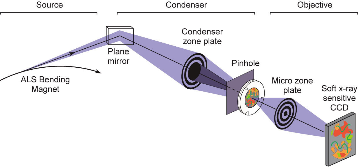
|
Characterization
of the spatial resolution of the microscope is
an important and active project in our group.
Here, we use the following definition of resolution:
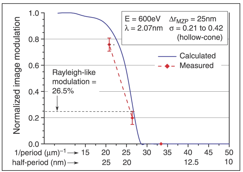
Res
= half-period of a equal line and space pattern
that exhibits Rayleigh-like 26.5% modulation in
its image
The
resolution, in general, can be expressed as  . .
 is the radiation wavelength, and NA is the numerical
aperture of the imaging optic.
is the radiation wavelength, and NA is the numerical
aperture of the imaging optic.  is a constant which primarily depends on the degree
of partial coherence of the illumination,
is a constant which primarily depends on the degree
of partial coherence of the illumination,  .
In our case, NA is equal to .
In our case, NA is equal to  ,
where ,
where  is the outermost zone width of the micro zone
plate. Thus,
is the outermost zone width of the micro zone
plate. Thus,
Res
= 
The
degree of partial coherence of the microscope,
,
is equal to . .
 is the outermost zone width of the condenser zone
plate (CZP). Typically,
is from 0.4 to 0.7, and
from 0.6 to 0.8. The resolution of the full-field
microscope is slightly finer than the smallest
zone width of the micro zone plate.
is the outermost zone width of the condenser zone
plate (CZP). Typically,
is from 0.4 to 0.7, and
from 0.6 to 0.8. The resolution of the full-field
microscope is slightly finer than the smallest
zone width of the micro zone plate.
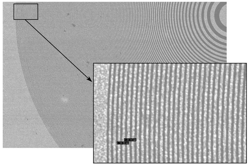
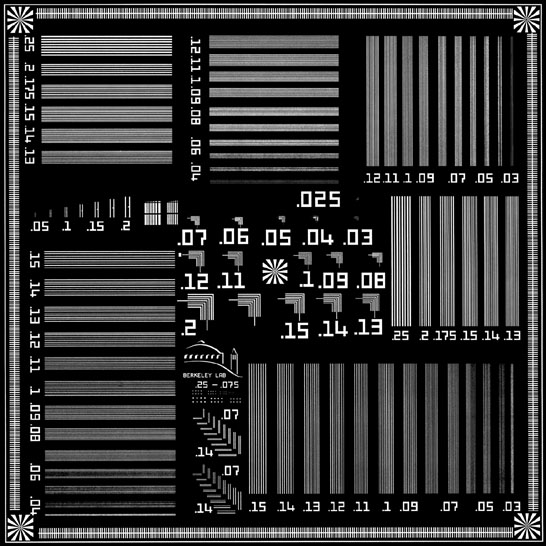
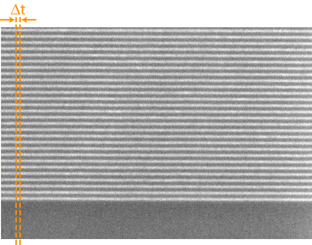
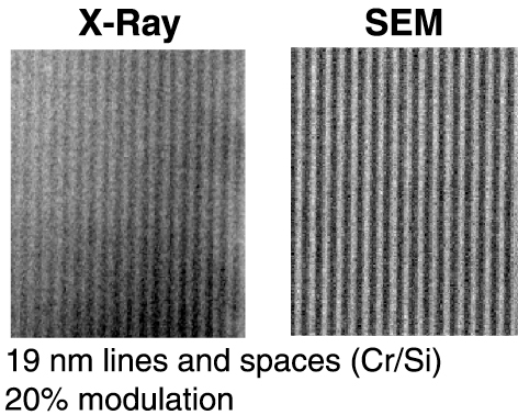
We design and fabricate various test objects for
measurement of the microscope’s resolution.
Test objects and measurement result are discussed
below.
|